【スーパーDEAL ポイント最大35%バック】ワッフル ケーキ 10個 | お菓子 洋菓子 詰め合わせ ギフト 個包装 クリスマス 内祝い お歳暮 御歳暮 ワッフルケーキ スイーツ 冷凍 秋…view page
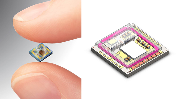
Intel is Bringing Silicon Photonics to the Data Center
view page
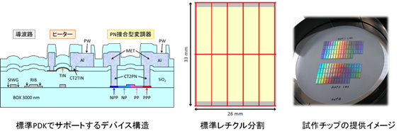
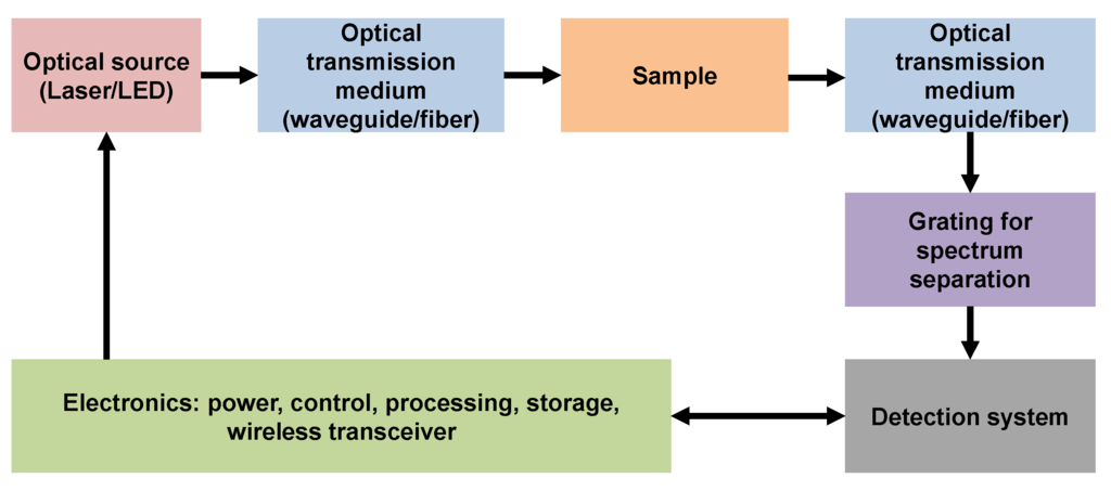
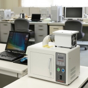
Silicon Photonics Test Systemsオンウエハ・シリコンフォトニクス・デバイス特性測定
view page
\スーパーSALE限定50%OFF/シーリングライト 照明器具 LED 調光調色 おしゃれ 電気 北欧 照明 6畳 8畳 10畳 12畳 14畳 リモコン付き LED対応 インテリア 間接照明…view page
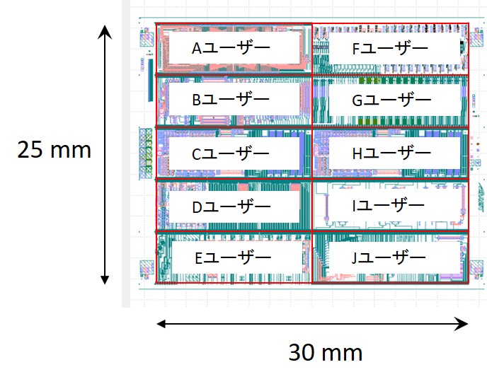
I-PEX、シリコンフォトニクスICを使用したアクティブ光モジュールのサンプル供給を開始
view page
Assembly and Design Solutions for Silicon Photonics, LiDAR, SiP, MCM Modules, IoT Sensors, Medical, Telecom, 5G RF and Commercial Applications.
view page
Silicon Photonics and 2.5D Interposer Design
view page
【スーパーSALE限定★61%OFF!】 電動自転車 a01 折りたたみ 電動アシスト自転車 erway 自転車 電気自転車 パワフル 5段階アシスト搭載 20インチ 7段変速 おしゃれ スポーツ…view page
Silicon Germanium SiGe Nanostructures
view page
Materials Integrated with Silicon Photonics Manipulate Light Phase at Low Loss
view page
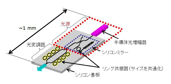
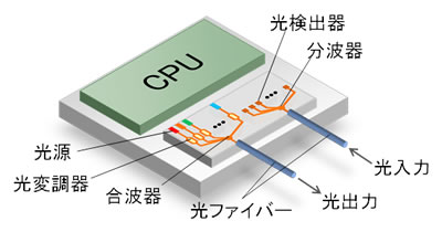
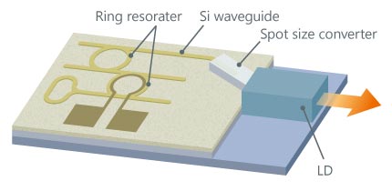
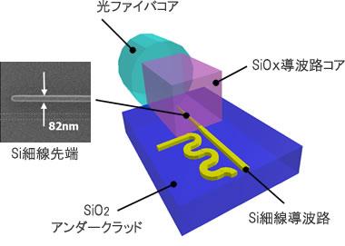
CPU間の大容量光インターコネクトに向けて小型のシリコンフォトニクス光源を開発
view page
【無料★特典付】 【特別価格】水受けセット ユニソン スプレスタンド60ソリッド 蛇口1個セット+ステンレスパン 蛇口付き立水栓 水栓柱&ガーデンパン 組合せセット 4カラー 1口水栓柱…view page
A schematic of a photonic integrated circuit with the different optical components labeled. Diode, Fiber Optic, Circuit, Optical, Components, Tech, Save, Blog, Quick
view page
【動画公開中】第一回公開講座「情報通信の歴史と未来を拓く新技術~シリコンフォトニクス~」
view page
What Is Silicon Photonics? | Intel Business
view page
【スペシャルSALE|クーポン配布】ガスコンロ リンナイ ガステーブル パールクリスタル ホワイト 白 59cm 両面焼きグリル プロパン 都市ガス 据置型ガスコンロ 2口 ココットプレート同梱…view page
OptoVue Pro– Enables Singulated Die Edge Coupling of Silicon Photonics Devices
view page
Silicon photonics meets the foundry
view page
【スーパーSALE限定★64%OFF~!】 サスペンション搭載 型式認定済 電動自転車 免許不要 130km走行可能 a02 折りたたみ 電動アシスト自転車 20インチ 自転車 350Wモーター…view page
期間値引クーポンあり ドレッサー おしゃれ 女優ミラー《自社製品》可愛い デスク 欧風 鏡台 お姫系 ベロア調 テーブル 幅80cm 幅60cm 幅100cm チェスト スツール LEDミラー…view page
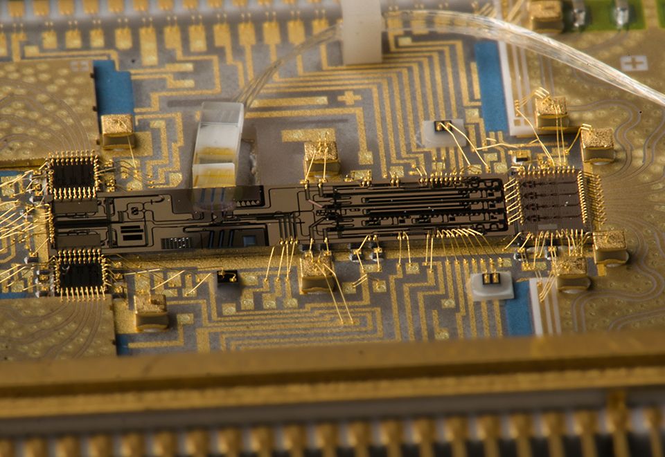
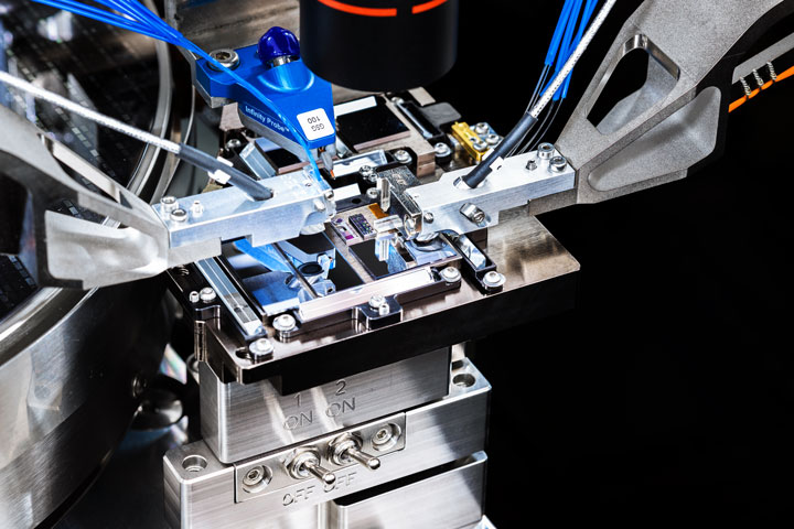
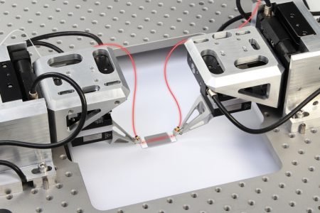
Automatic Silicon Photonics Packaging Systems from ficonTEC
view page
シリコンフォトニクス技術による光電融合型光送受信モジュールの開発NTTデバイスイノベーションセンタ
view page
眩しくない 鯖江 夜間 運転 サングラス 運転用 調光サングラス レディース ネオコントラスト 調光 ナイト おしゃれ ボストン メガネ メラニン uvカット 白内障 術後 保護メガネ ネオグラス…view page
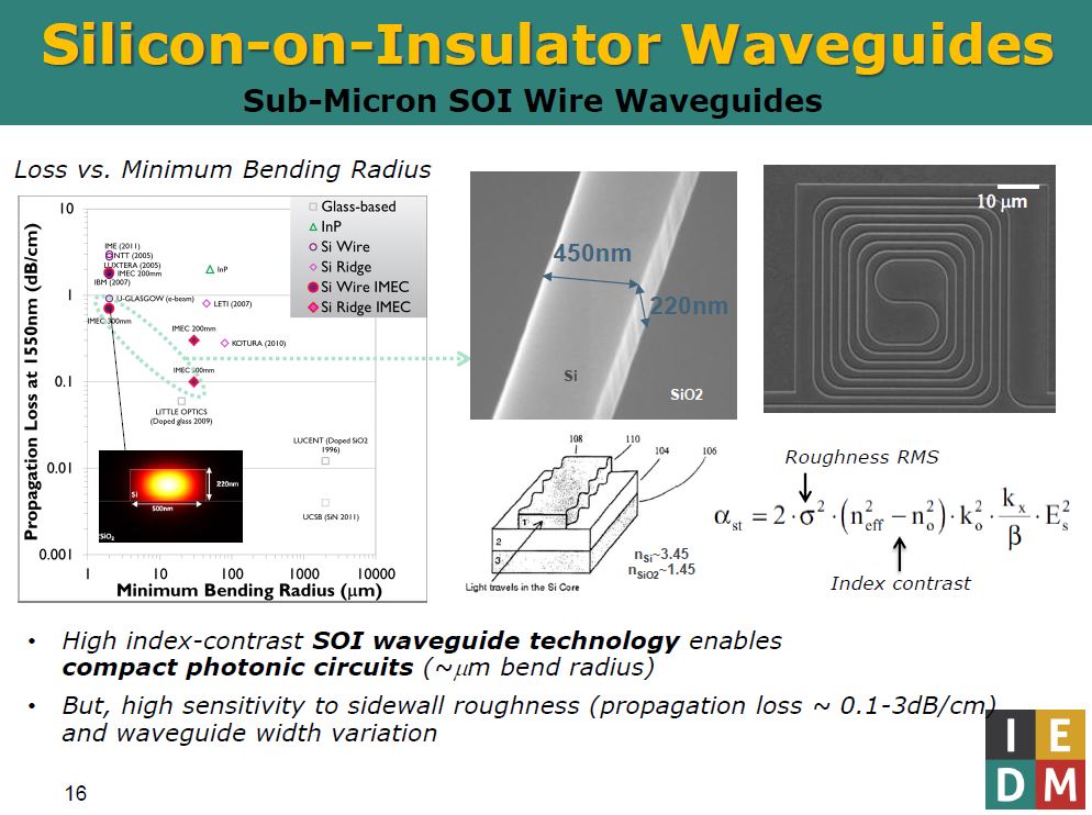
シリコン光導波路と基本的な光波長フィルター:福田昭のデバイス通信(147) imecが語る最新のシリコンフォトニクス技術(7)(2/2 ページ)
view page
ASE lands Broadcom orders for silicon photonics-based networking chips
view page
お歳暮 お菓子 ギフト スイーツ クッキー 詰め合わせ 御歳暮 冬ギフト 高級 おしゃれ 誕生日プレゼント 個包装 がらんの小石 30個入 お取り寄せスイーツ プチギフト 焼き菓子 出産祝い…view page
Silicon Photonics: Fundamentals and Devices
view page
Low-Temperature Bonding for Silicon-Based Micro-Optical Systems
view page
【納期お問合せ下さい】 UNISON ガーデンシンク バル 立水栓 バルスタンド トールポット 上下蛇口 セット BARU 水栓柱 ユニソン 補助蛇口 ホース用 2口 ガーデンポット サテン…view page
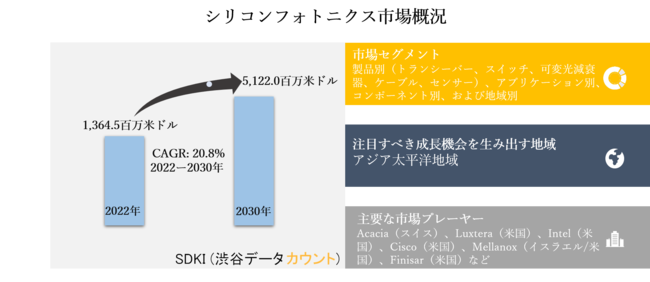
シリコンフォトニクス市場ー製品別(トランシーバー、スイッチ、可変光減衰器、ケーブル、センサー)、アプリケーション別、コンポーネント別、および地域別ー世界的な予測2030年
view page
半導体レーザーとシリコン光導波路を接続する技術(前編):福田昭のデバイス通信(158) imecが語る最新のシリコンフォトニクス技術(18)(2/2 ページ)
view page
光ファイバーとシリコン光導波路を結合する技術:福田昭のデバイス通信(157) imecが語る最新のシリコンフォトニクス技術(17)(1/2 ページ)
view page
49%OFF!【12/9限定:1,876円!クーポン利用で】スマホケース iphone16 ケース iphone15 ケース iphoneケース iphone16e ケース スマホショルダー…view page
Silicon Photonics, Simultaneous Testing of Optical Components
view page
Silicon Photonics Test Systemsオンウエハ・シリコンフォトニクス・デバイス特性測定
view page
応接セット 4点セット 4人 応接 ソファ 椅子 応接テーブル ソファセット 応接室 おしゃれ モダン 会議セット 商談 オフィス コンパクト シャルマン SA681-2-T13Sview page
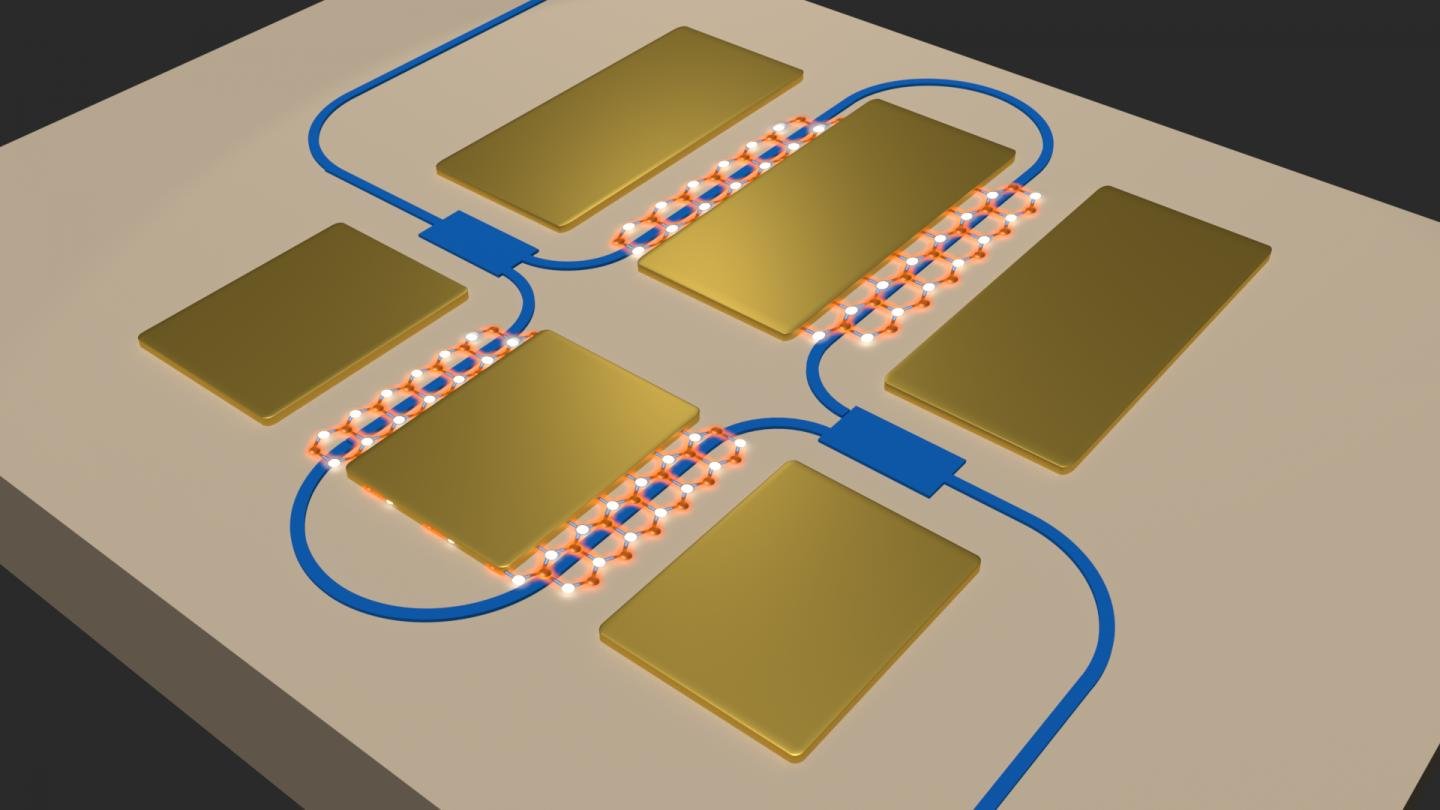
Optical Logic Gates Based on Z-Shaped Silicon Waveguides at 1.55 μm
view page
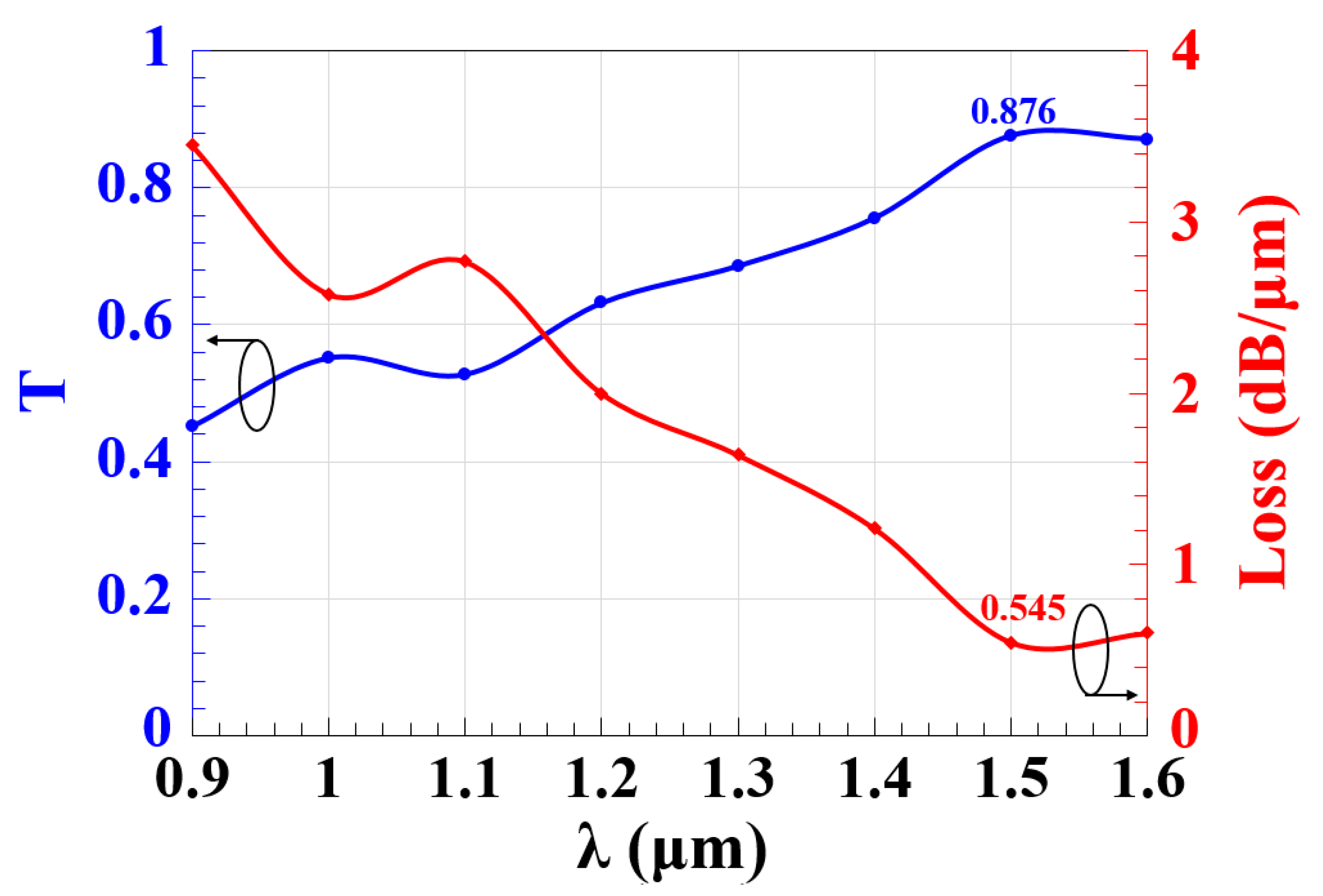
Rare Earth-Doped Silicon-Based Light Emitting Devices
view page
ペーパーポット ティッシュケース おしゃれ トイレットペーパー対応 ティッシュホルダー ティッシュカバー かわいい 丸型 ボックスティッシュ対応 Aicollection アイコレクション 日本製…view page
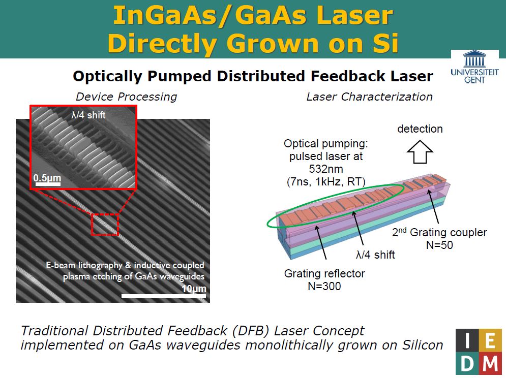
化合物レーザーをシリコンにモノリシック集積する試み(後編):福田昭のデバイス通信(167) imecが語る最新のシリコンフォトニクス技術(27)(1/2 ページ)
view page