Category:半導体製造

シリコンウェハー
レジスト
Resist (semiconductor fabrication)
半導体製造装置

ファウンドリ
Foundry model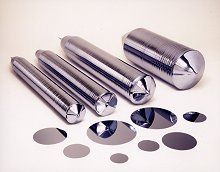
チョクラルスキー法
Czochralski method
エッチング
Etching
ナノインプリント・リソグラフィ
Nanoimprint lithography
ミニマルファブ

スパッタリング
Sputtering
有機金属気相成長法
Metalorganic vapour-phase epitaxy
System-on-a-chip
System on a chip半導体デバイス製造
Semiconductor device fabrication
熱酸化
Thermal oxidationメゾスコピック領域
Mesoscopic physics
反応性イオンエッチング
Reactive-ion etching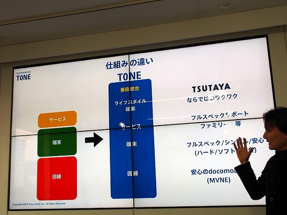
垂直統合型デバイスメーカー
Integrated device manufacturer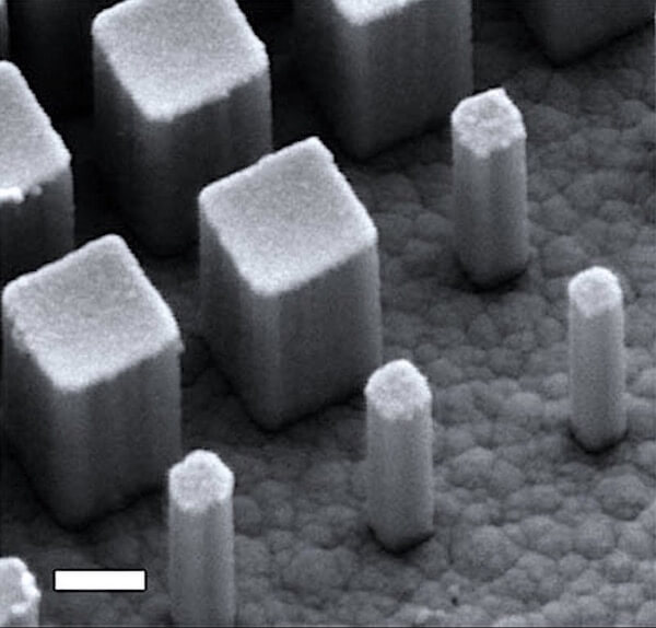
集束イオンビーム
Focused ion beam
ベーキング
Low hydrogen annealingSiP
System in a packageサリサイド
Salicide
テスト対象デバイス
Device under test
ダイボンダ
ラピッドサーマルプロセス
Rapid thermal processing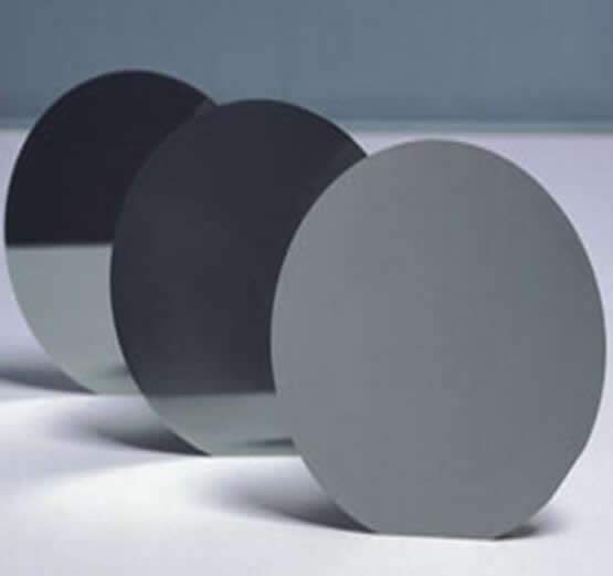
ウェハー
Wafer (electronics)
ホウリンケイ酸ガラス
Borophosphosilicate glass
自己整合
スピンコート
Spin coating
テープアウト
Tape-out